Bend Radius for a PCB Flex Circuit
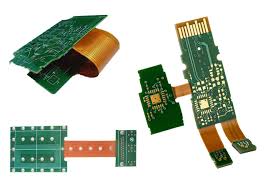
PCB flex circuits are vital components in many electrical design applications. The flexibility of these printed circuit boards allows them to bend and flex to accommodate the unique dimensions of a finished product, which provides significant space savings over traditional rigid boards. But working with a flex ribbon can create unique challenges, especially when it comes to determining the correct minimum bend radius. This is because excessive bending can damage or shorten the life of the circuit board. The goal is to ensure that conductive traces and other components remain intact during the bending process.
To achieve this, it is critical to properly design a flex circuit and follow appropriate guidelines. For example, excessive bending with a tight radius (a small multiple of the substrate thickness) can cause copper trace fracture, dielectric delamination, and other problems that could reduce performance and reliability. To prevent these issues, it is essential to follow proper bending guidelines and use mechanical testing and verification.
The recommended minimum bend radius for a pcb flex depends on the type of flex and construction, so it is important to consult with a reputable PCB manufacturer to get more specific guidelines. However, a few general rules can help. For example, a multi-layer flex circuit with a thicker copper thickness and single or double-sided construction should have a minimum bending radius of 10X the thickness of the substrate.
Calculating the Bend Radius for a PCB Flex Circuit
It is also important to consider the insulating material used in a flex circuit. While PI and PET films are common for flexible circuits, thin glass fiber or epoxy cores can also be used for more complex designs. In addition, the circuits should have a coverlay or laminate on the outer surface to protect it from corrosion and other damage.
The best way to calculate the minimum bending radius for a PCB flex is using a computer program that uses a finite element analysis to model the stress distribution in the structure, taking into account the specific materials and layer stackup. This is a more time-consuming approach but offers greater accuracy than simple formulas.
The durability of PCB flex is another key benefit, especially in applications where reliability is paramount. Unlike rigid PCBs, which are susceptible to mechanical stress and vibration, flexible circuits can withstand bending, twisting, and even folding without compromising their electrical integrity. This durability makes PCB flex ideal for use in harsh environments where traditional electronics would falter, such as automotive interiors, aerospace systems, and wearable devices.
In addition to calculating the minimum bend radius, it is also helpful to use mechanical testing and verification on a physical prototype to identify potential issues with folding, alignment, and component interference. Finally, it is necessary to determine how any folded areas will be attached to the rest of the flex circuit in order to distribute stress and provide mechanical support.